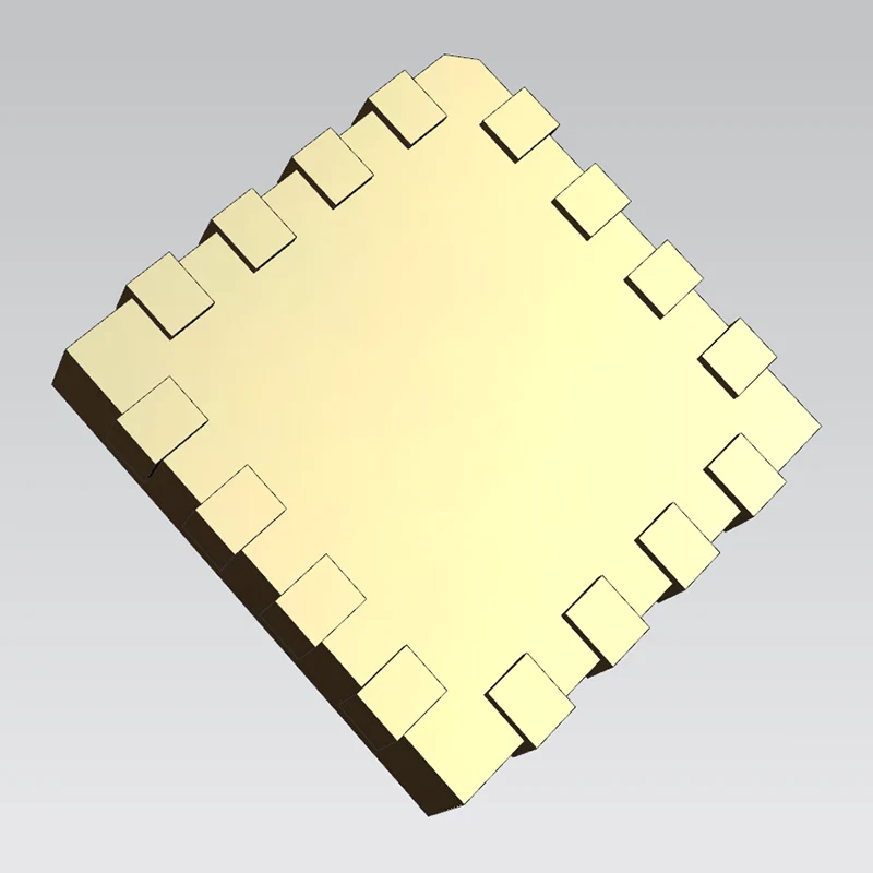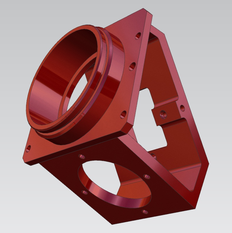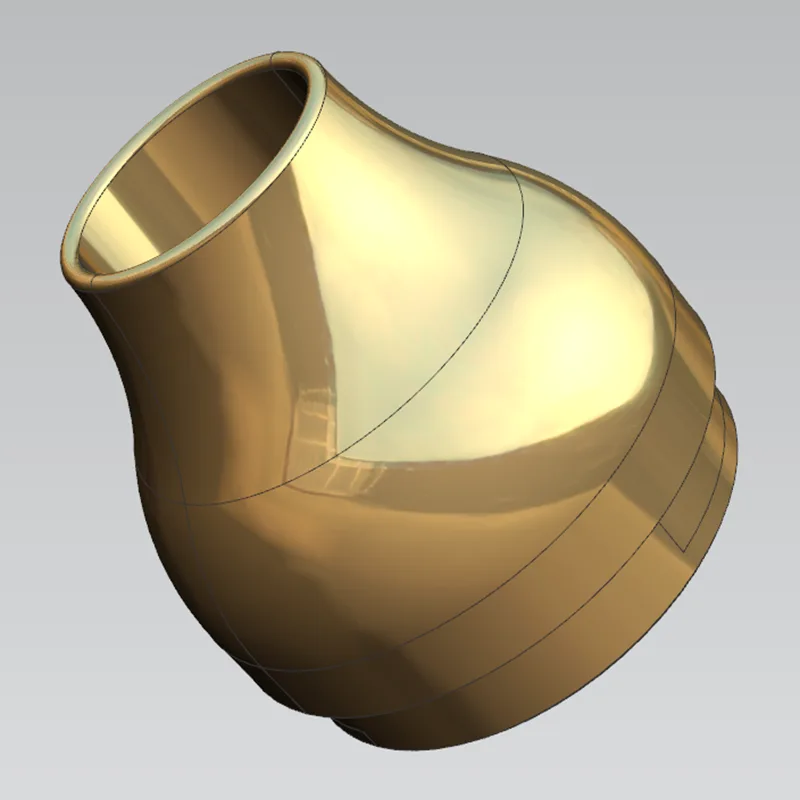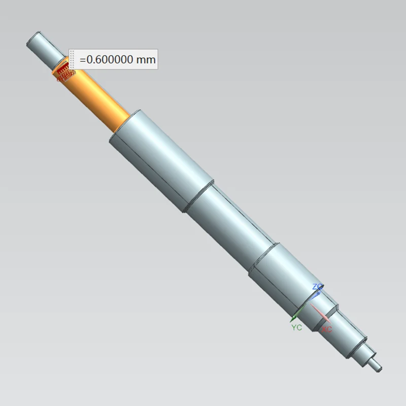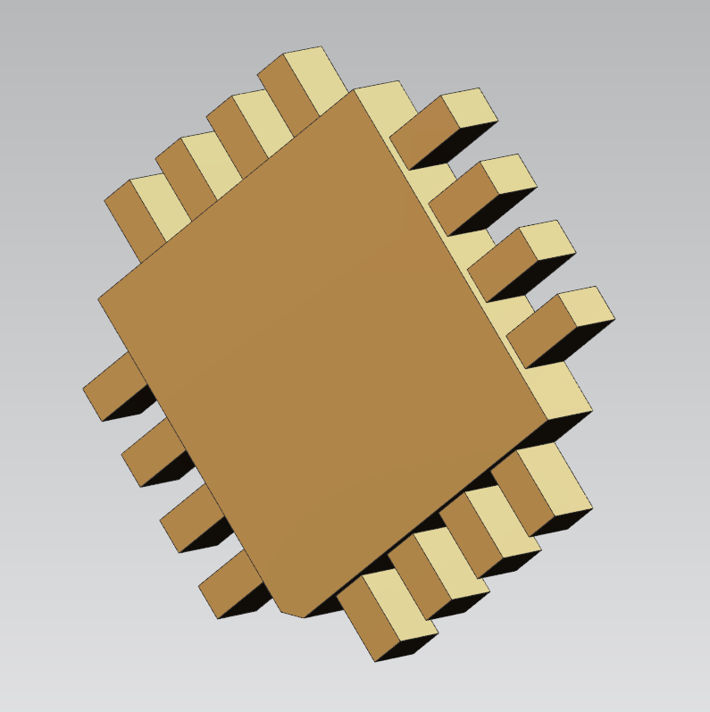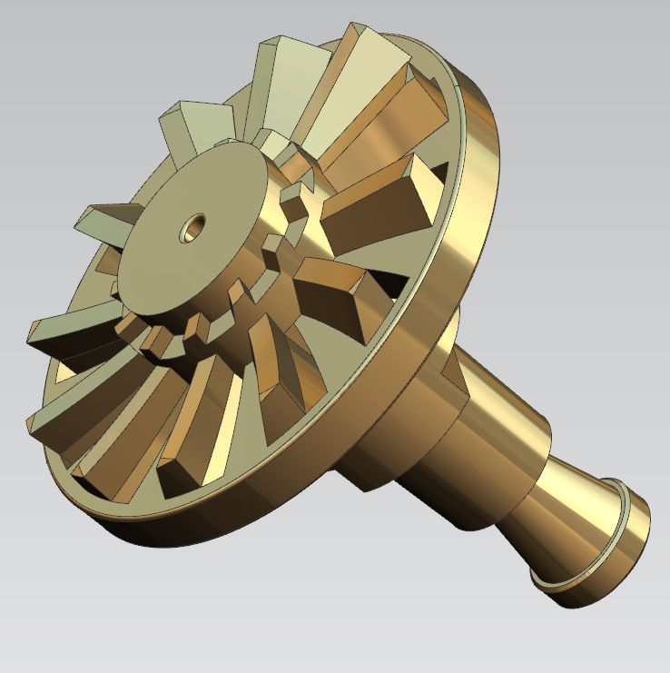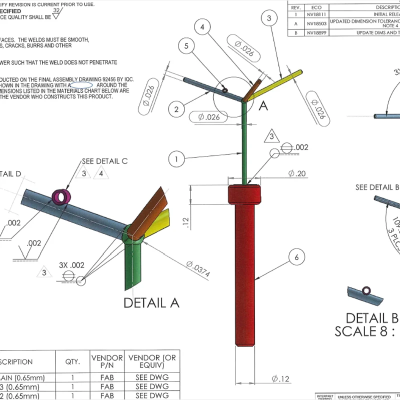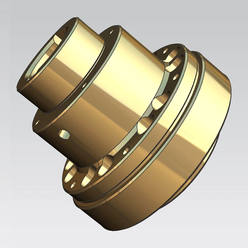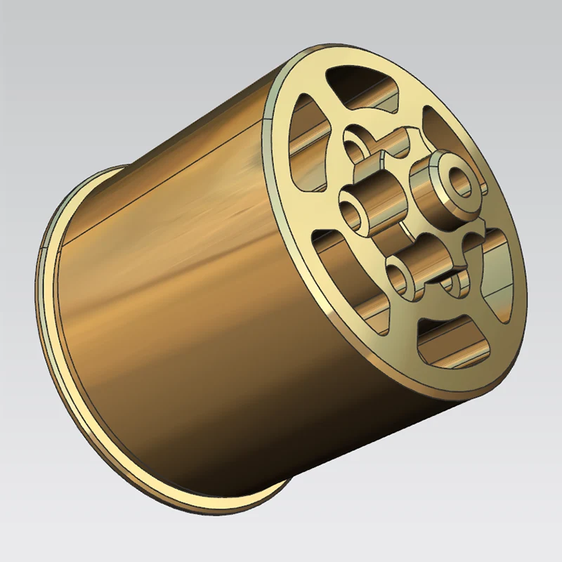
Our semiconductor precision machining process for advanced applications is engineered to meet the extraordinary demands of modern chip manufacturing, where nanometer-level accuracy and particulate-free cleanliness are non-negotiable.
The semiconductor industry demands some of the most precise components ever manufactured, where even sub-micron errors can render entire wafers useless. We provide critical components that support multiple stages of semiconductor manufacturing.
We manufacture precision components used directly in wafer processing equipment, where dimensional accuracy and surface quality directly impact yield and performance.
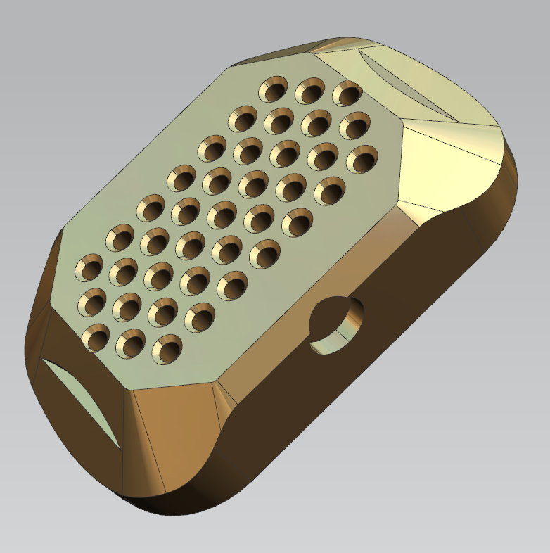
1. Wafer chucks: Precision vacuum and mechanical chucks with flatness of 0.001mm and vacuum adsorption force uniformity of ±1% for secure, damage-free wafer handling.
2. Diamond grinding knives: Precision diamond-tipped tools for silicon wafer grinding and thinning processes.
3. Coating fixtures: Precision fixtures for thin-film deposition and coating processes used in semiconductor manufacturing.
We also produce components for semiconductor packaging and assembly equipment, supporting the back-end of the chip manufacturing process.
1. Vacuum fixtures: Precision vacuum handling components for die attach and packaging processes.
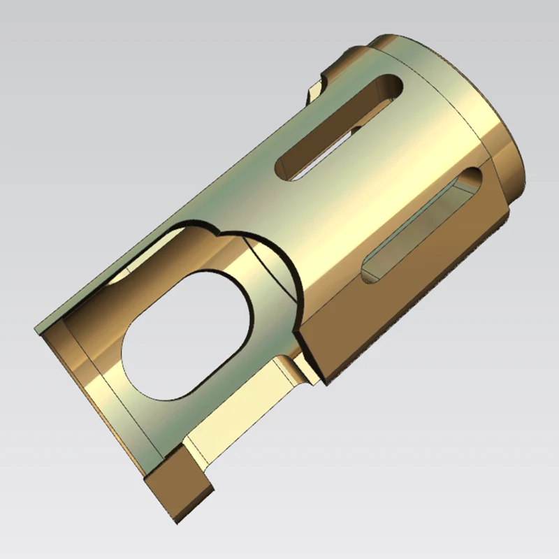
2. Elastic supports: Compliant mounting structures that provide stable support while accommodating thermal expansion.
3. Precision tooling: Custom tooling for semiconductor assembly and testing operations.
The semiconductor precision machining process for advanced applications we have developed combines multiple complementary technologies to achieve the levels of accuracy and cleanliness that semiconductor manufacturing demands.
Manufacturing semiconductor-grade precision components requires a carefully controlled process that maintains accuracy and cleanliness from raw material through final inspection.
Our semiconductor component manufacturing follows a rigorous multi-stage process designed to achieve the highest levels of precision and quality.
1. Material selection: Careful sourcing and inspection of raw materials suitable for semiconductor environments.
2. Rough machining: Initial material removal with conventional tools, leaving controlled stock for precision finishing.
3. Heat treatment: Vacuum heat treatment for stress relief and material property optimization.
4. Precision machining: Fine machining on ultra-precision equipment to achieve final dimensions and tolerances.
5. Surface finishing: Polishing, coating, or other surface treatments as required by the application.
6. Cleanroom assembly: Final assembly and inspection in controlled clean environments.
We maintain tight process control throughout manufacturing to ensure consistent quality across every semiconductor component we produce.
1. In-process inspection: Regular dimensional checks at key process stages to catch deviations early.
2. Statistical process control: Monitoring of critical process parameters to maintain stability and predictability.
3. Traceability: Complete traceability of materials, processes, and inspections for every component.
Components used at the wafer level of semiconductor manufacturing require the highest levels of flatness, parallelism, and surface quality to ensure uniform processing across entire wafers.
Wafer-level components must maintain extraordinary flatness to ensure uniform contact and processing across the entire wafer surface.
1. Surface flatness: Achieving flatness as tight as 0.0003mm on critical wafer contact surfaces.
2. Parallelism: Maintaining parallelism of 0.001mm between opposing surfaces of wafer handling components.
3. Surface roughness: Ultra-smooth surfaces with roughness as low as Ra0.05μm to prevent wafer scratching and contamination.
Many semiconductor components incorporate vacuum channels or fluid passages that require precise machining and leak-free performance.
1. Micro-channel machining: Precision machining of tiny vacuum and fluid channels in wafer chucks and manifolds.
2. Sealing surfaces: Ultra-flat sealing surfaces for reliable vacuum and fluid sealing.
3. Force uniformity: Vacuum adsorption force uniformity of ±1% across the entire wafer contact area.
Semiconductor components must be manufactured and handled in controlled environments to prevent particulate contamination that could damage delicate semiconductor devices.
We maintain dedicated clean manufacturing spaces for semiconductor component production and assembly.
1. Cleanliness level: Class 1000 dust-free clean rooms for critical semiconductor component processing.
2. Temperature control: Constant temperature maintained at ±0.5°C to ensure dimensional stability during precision machining.
3. Humidity control: Regulated at 40-60% to prevent static discharge and material moisture absorption.
Semiconductor-grade precision machining is extremely sensitive to vibration, which can cause surface defects and dimensional errors on ultra-precision components.
1. Anti-vibration foundations: Specialized machine foundations with vibration amplitude below 0.1μm.
2. Active isolation: Active vibration isolation systems on our most precise semiconductor manufacturing equipment.
3. Facility layout: Careful factory layout to minimize vibration transmission between different process areas.
Quality assurance is an integral part of our semiconductor precision machining process for advanced applications, with checkpoints built into every stage of production to ensure compliance with the highest industry standards.
Quality is paramount in semiconductor manufacturing, where component failures can lead to millions of dollars in lost production. Our quality systems are designed to ensure the highest levels of reliability.
Our quality management system is certified to international standards and continuously refined for semiconductor industry requirements.
1. ISO9001:2008: Quality management system certification ensuring consistent product quality and process control.
2. ISO14001:2004: Environmental management system certification reflecting our commitment to sustainable manufacturing.
3. National standards: Products manufactured to the national standard of China, with additional customer-specific requirements as needed.
We maintain an extensive array of inspection equipment to verify every critical characteristic of our semiconductor components.
1. Coordinate measurement: Automatic three-coordinate measuring machines for comprehensive 3D dimensional verification.
2. Optical inspection: Image analyzers, projectors, and high-power microscopes for surface and feature inspection.
3. Surface measurement: Roughness testers, flatness gauges, and profilometers for surface quality verification.
4. Precision tools: Height gauges, micrometers, and ten-thousandth meters for precise dimensional checks.
Our semiconductor component manufacturing is supported by advanced ultra-precision equipment platforms capable of achieving the tight tolerances the industry demands.
|
Parameter Category |
Parameter Details |
|
Equipment Model |
UPL 150 |
|
Core Positioning |
Ultra-precision milling and turning composite machining |
|
Axis Number |
4-axis (X, Y, Z, C) |
|
Key Accuracy |
Machining accuracy ±0.0001mm, surface roughness Ra0.01μm |
|
Spindle System |
High-speed air-bearing spindle, maximum speed 80,000 rpm |
|
Structural Features |
Granite bed, active vibration isolation system |
|
CNC System |
Siemens 840D sl |
|
Typical Application |
ultra high precision machining of micro-components, precision sensors |
A: We produce a wide range of precision components for the semiconductor industry including wafer chucks, vacuum fixtures, coating fixtures, diamond silicon wafer grinding knives, elastic supports, and various precision tooling for semiconductor manufacturing and packaging equipment.
A: We maintain Class 1000 dust-free clean rooms for semiconductor component processing and assembly. Our facilities also include constant temperature control at ±0.5°C, humidity regulation between 40-60%, and anti-vibration foundations to support the ultra-precision requirements of semiconductor manufacturing.
A: We can achieve flatness as tight as 0.0003mm on critical wafer contact surfaces, with standard wafer chuck flatness of 0.001mm. We also maintain vacuum adsorption force uniformity of ±1% across the entire wafer contact area for consistent, damage-free wafer handling.
A: We process a wide range of materials suitable for semiconductor applications including various stainless steels, aluminum alloys, titanium alloys, ceramics, optical glass, quartz, and engineering plastics such as PEEK, PEI, PAI, and UPE. Material selection depends on the specific application requirements.
A: Yes, we support minimum order quantities of just 1 piece for prototype development and can scale to production volumes of 999,999+ pieces. We work with both R&D teams developing new semiconductor processes and production teams requiring high-volume component supply.
A: We have implemented and obtained ISO9001:2008 and ISO14001:2004 quality system standards certifications. We also maintain a 16-person quality management team including QE, IQC, IPQC, and OQC specialists, with over 320 units of inspection equipment to verify every critical dimension.
Partnership Value
Sanluo Precision stands as a reliable partner for semiconductor precision machining process solutions for advanced applications, combining 18+ years of industry experience with state-of-the-art equipment and cleanroom manufacturing capabilities. Our ability to produce wafer chucks with 0.001mm flatness, vacuum fixtures with ±1% force uniformity, and precision tooling for semiconductor manufacturing has earned the trust of leading companies in the industry. With ISO-certified quality systems, 130+ production machines, and a team of 230+ skilled professionals, we have the scale and expertise to support your most demanding semiconductor component requirements. From prototype development to high-volume production, we deliver the precision, cleanliness, and reliability that semiconductor manufacturing demands.